Affordable, high-precision 3D printed unalloyed copper parts from Holo are driving advances in next-gen thermal and electrical systems
Key Points
- High purity copper is required to build components with high thermal and electrical conductivity. Small differences in purity can have large performance ramifications.
- The ability to 3D print small, intricate, copper structures can drive thermal and electrical performance via higher surface area to volume ratio features and increased packing density
- Copper thermal devices printed by Holo have exceeded the performance of traditional manufacturing methods
Copper is an incredible engineering material that underpins many advanced thermal and electrical systems, but it also presents unique challenges to manufacturing as those systems become smaller and more complex over time. The design of advanced copper components is often driven by computer simulations in advanced physics fields like thermodynamics and heat transfer, radio frequency (RF) engineering, and electronics theory, which sets copper apart from the aluminums and steels often used in more mechanical or structural applications. Simulation offers insight into theoretical best case copper component designs, but traditional manufacturing methods often struggle to create those geometries, and that leaves performance on the table.
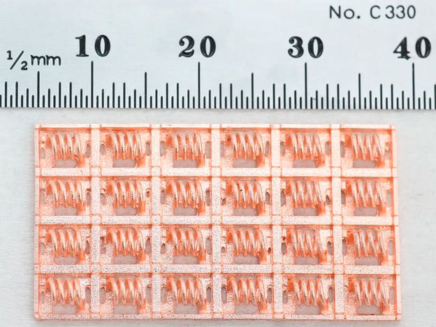
A custom array of inductors printed with Holo’s PureForm metal AM process
Pure, unalloyed copper can be a tricky material to work with — it’s ductile, and parts with thin features can easily deform during CNC machining. Advanced additive manufacturing (AM) technologies that can handle intricate part geometries often use alloyed copper materials to improve printability, but at a high cost to pure copper’s attractive thermal and electrical properties. Some newer powder bed fusion (PBF) technologies have been designed specifically for pure copper, but they require expensive, dedicated machines and facilities. The ideal solution is a cost-effective combination of the geometric capabilities of 3D printing, with the functional material properties that make pure copper valuable in engineering applications.
Holo’s PureForm™ metal 3D printing service gives electrical, thermal, and RF engineers the tools to explore geometries and applications that they couldn’t previously even imagine building. We can deliver highly intricate, pure copper components quickly and without the high capital investment costs of on-site metal AM technologies, and PureForm parts have outperformed traditionally manufactured ones. Let’s take a look at how that works.
A small but mighty addition to your design toolbox
The PureForm process enables you to quickly develop pure copper components, in complex, intricate geometries, at tiny scales. What can that design freedom help you achieve?
From an electrical standpoint, 3D printing pure copper unlocks the ability to quickly customize all kinds of RF and power transmission applications, like antennas, waveguides, intricate interconnects, connector pins, miniature inductors, distributors, bus bars, and more. Ongoing electrification R&D efforts in the automotive and aerospace industries have also driven demand for complex new copper components in battery management and power distribution systems. 3D printing these parts can increase the pace of product development, even for copper components that may be eventually cast or machined in production.
The high degree of control over part geometry delivered by the PureForm printing process also empowers you to create all kinds of unconventional thermal management designs, for custom heat exchangers, liquid cold plates, and heatsinks for spatially-constrained applications.
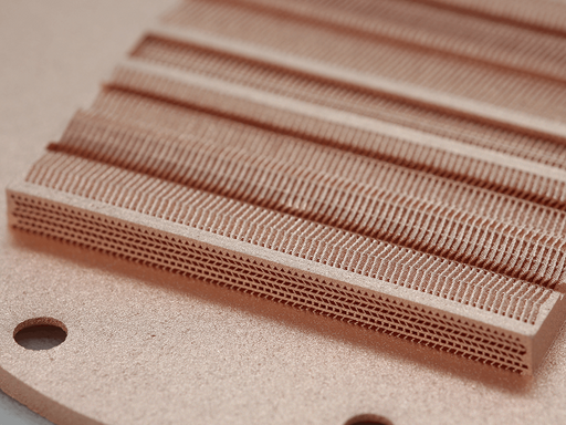
Close-up view of the intricate fins in a high-performance liquid cold plate application printed with the PureForm process
When it comes to thermal and electrical components, system performance is often inversely proportional to minimum feature size. Heat exchangers like cold plates can benefit from tiny features or textures that induce turbulence and increase the surface area to volume ratio of the heat transfer interface. Inductors and other electrical components can be created with more complex geometries in equal or smaller volumes, and that can drive higher packing density and increased performance.
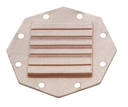
A liquid cold plate with complex turbulence-inducing features printed by Holo
As an example, we’ve developed a number of microchip cold plate applications with substantially higher cooling performance than a traditionally manufactured version that employed micro-skived straight channels. Skiving can only produce fairly limited, straight channel geometries, which limits the flexibility of the designer to tailor the cold plate to the thermal application. By contrast, printing the plate with our PureForm process allowed us to create much more surface area in the fluid interface, and customize the cooling performance in different zones of the plate. Not only did this improve the ability to pull more heat out of the chip, but it also means that cooling could be better localized to the specific regions where heat was generated.
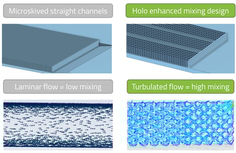
The complex flow paths of the Holo designed cold plate (right) encourage turbulent fluid flow which promotes a high degree of mixing, and better heat transfer performance than the traditional skived design (left)
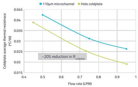
Performance of the Holo printed cold plate versus a traditionally manufactured (micro-skived) version. The printed component exhibited a roughly 20% reduction in thermal resistance, which translates to a significantly improved capacity to transfer heat through the cold plate
If you’re employing lengthy computer simulations like computational fluid dynamics (CFD) to develop your copper component designs, you can parallelize those efforts with the ability to quickly 3D print a wide array of designs to accelerate your R&D process. In one case, we partnered with a customer designing custom thermal management solutions to help them design, build, and test twelve different prototypes within a week. The analytical simulations for those same, highly complex designs took almost four weeks to complete, which meant that this manufacturer had real world performance data in hand to help drive their engineering strategy almost a month earlier.
The technical details
Copper purity is essential to the material’s high thermal and electrical conductivity. Because of copper’s strong ability to reflect light, 3D printing processes that build copper parts with lasers, such as direct metal laser sintering (DMLS), often use alloying elements to reduce reflectance and improve its printability. From an electrical conductivity perspective, alloying elements act similar to impurities and disrupt the flow of electrons through the metal, reducing the overall conductivity. This is why you should choose a 3D printing process that’s capable of building in pure, unalloyed copper if you’re looking to print copper parts for their electrical properties.
Holo’s PureForm metal 3D printing service can build pure copper components, with tiny, intricate features, much more cost-effectively than other 3D printing technologies that can produce similar parts. Copper parts created with the PureForm process will have these typical material properties:
|
Bulk density |
95% |
|
Electrical conductivity |
92% IACS |
|
Thermal conductivity |
92% copper standard |
How does the technology work?
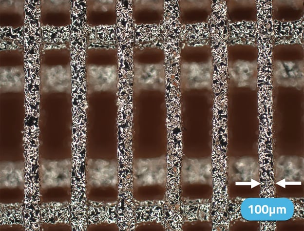
Holo’s PureForm process can produce intricate feature details as small as 100µm, which can be a powerful tool for increasing the surface area of copper parts to maximize their heat transfer capability
The PureForm process uses a combination of a digital projector-based metal-laden photopolymer 3D printing technology, paired with a metal injection molding (MIM) sintering step to create intricate, solid metal parts. Copper is a well-established MIM material (you can even buy MIM copper golf clubs!) and can achieve high thermal and electrical conductivities after sintering. Combining that with Holo’s high resolution photopolymer 3D printing process creates the capability to build highly detailed copper parts with the material properties that thermal and electrical applications demand.
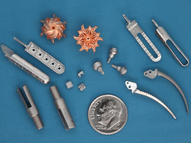
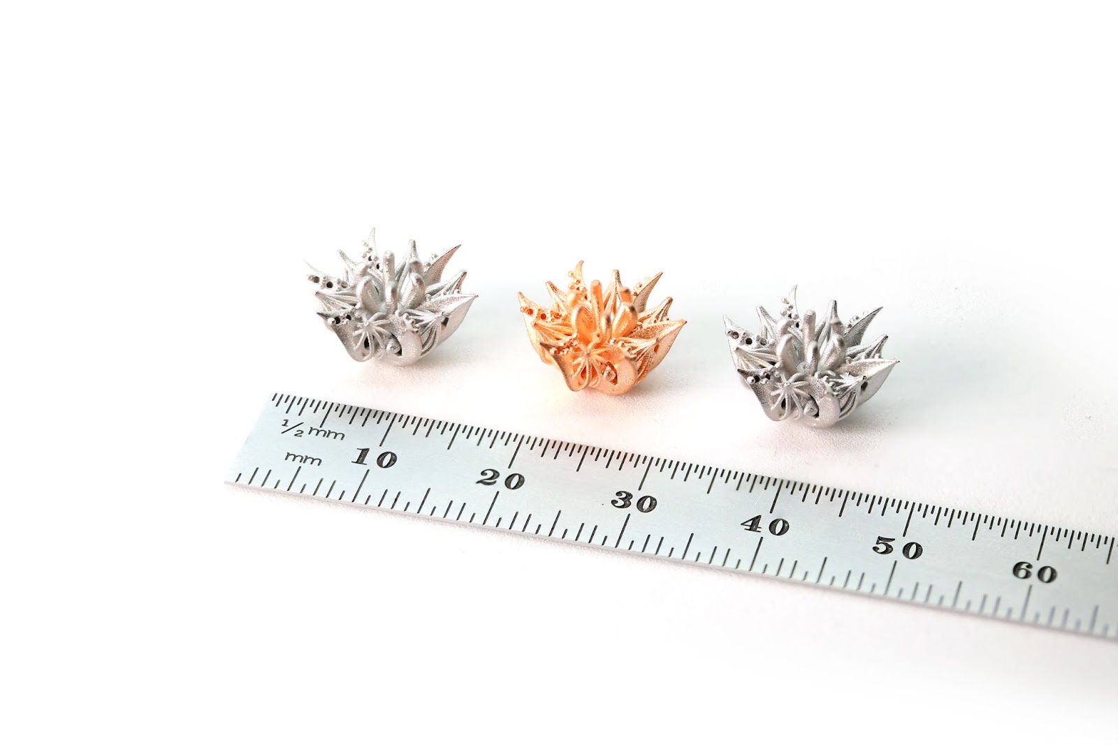
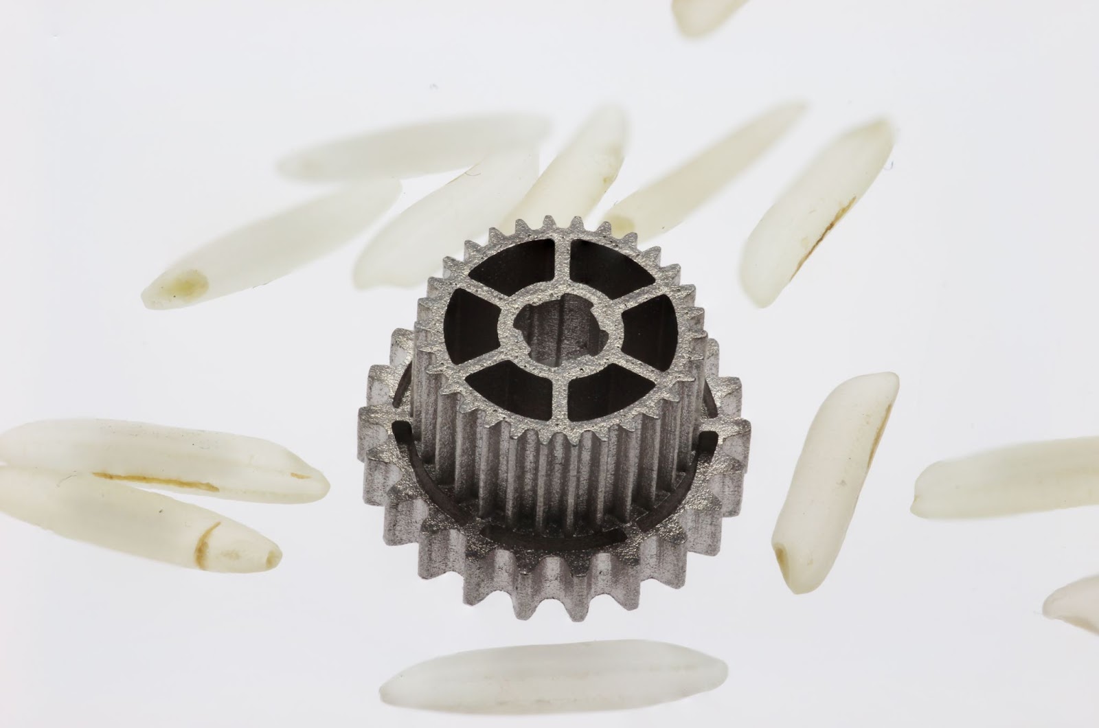
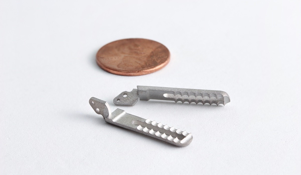
A selection of pure copper, stainless steel, and titanium parts manufactured with Holo’s PureForm 3D printing technology
—
Do you have a complex copper application you’d like to discuss with our engineering team? Drop us a line to request a project review and we’ll set up a time to chat!